What Happened
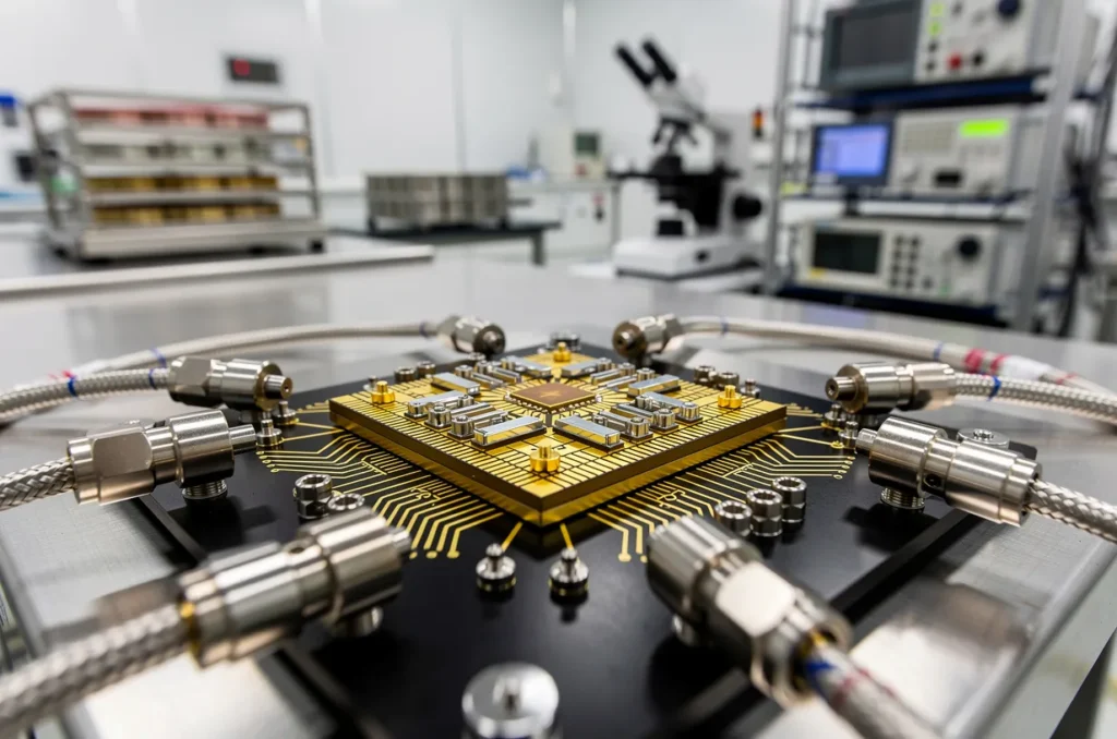
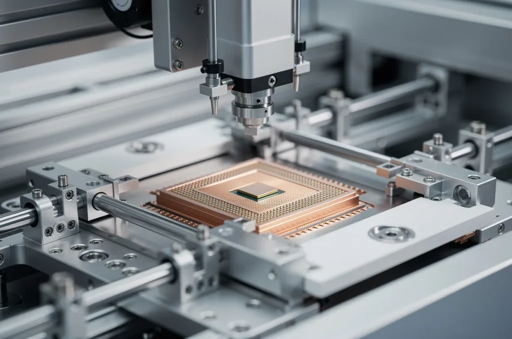
One of the most important bottlenecks in the AI chip race is no longer just chip fabrication. It is advanced packaging — the step where multiple chip components are connected, protected, and assembled into the final high-performance systems used in AI servers.
That matters because even some of the most advanced chips made in the United States still have to be shipped back to Taiwan for packaging before they are ready for use. As AI demand rises, that extra step is becoming more visible, more strategic, and more constrained.
Why Packaging Suddenly Matters So Much
For years, packaging was treated as a back-end manufacturing step. Now it is much closer to the center of the AI hardware story.
Modern GPUs and other accelerator chips are no longer simple, single-die products. They increasingly combine:
- logic chips
- high-bandwidth memory
- multiple interconnected dies
- denser links between compute and memory
That is where advanced packaging comes in. It allows those pieces to be combined into one larger system that can handle the performance, power, and efficiency demands of modern AI inference and training workloads.
In practical terms, packaging is no longer an afterthought. It is part of how leading chipmakers squeeze more performance out of silicon as traditional transistor scaling becomes harder.
TSMC Is Still The Packaging Volume Leader
TSMC remains the dominant player in advanced packaging, especially through its CoWoS technology. That platform is now deeply tied to the AI buildout, and demand has surged fast enough to create a fresh capacity squeeze.
According to the report, Nvidia has reserved the majority of TSMC’s most advanced packaging capacity. TSMC’s packaging head said the company’s most advanced method is growing at an 80% compound annual growth rate, which shows how quickly demand is expanding.
That helps explain why packaging is starting to look like the next constraint in the AI supply chain. If wafer output keeps rising but packaging does not scale alongside it, the bottleneck simply moves downstream.
Even Arizona Chips Still Make A Taiwan Round Trip
One of the clearest signs of the problem is geographic. Right now, TSMC sends 100% of its chips to Taiwan for packaging, including chips made at its advanced fab in Phoenix, Arizona.
That means a chip can be fabricated in the U.S., shipped to Asia for packaging, and then sent back to customers. The process adds time, logistics complexity, and another layer of reliance on overseas infrastructure.
TSMC is now building two packaging facilities in Arizona and ramping two more in Taiwan, but it has not disclosed a completion timeline for the U.S. sites.
For customers, local packaging capacity matters because it could reduce turnaround times and keep more of the production chain closer to the fab itself.
Intel Is Trying To Use Packaging As An Opening
Intel is the other major name in this story. While the company has struggled to land a major outside customer for its foundry manufacturing business, it has already attracted packaging customers such as Amazon and Cisco.
That matters because packaging may offer Intel a lower-friction way to deepen relationships with major AI customers before winning full fabrication business.
Intel’s advanced packaging work spans facilities in:
- New Mexico
- Oregon
- Chandler, Arizona
- and major final packaging operations in Vietnam, Malaysia, and China
The company’s leading packaging technology, EMIB, is positioned as an alternative to TSMC’s packaging approach. Intel argues it can deliver some cost advantages by embedding small silicon bridges only where they are needed.
Musk Adds Another Signal
The packaging story also got a boost from Elon Musk, who tapped Intel to package custom chips for SpaceX, xAI, and Tesla tied to his planned Terafab project in Texas.
That is notable because it suggests packaging is becoming a strategic selling point in its own right, not just a support function behind fabrication.
It also reinforces a broader idea now circulating in the sector: some customers may be willing to work with Intel on packaging first, then potentially expand into foundry relationships later.
The Real Constraint Is Performance Density
The reason all of this matters is that AI performance gains increasingly depend on how efficiently chip components are connected.
Traditional 2D packaging works for simpler chips like many CPUs. But more advanced systems, especially GPUs, need tighter and faster communication between compute and memory.
That has pushed the industry toward:
- 2.5D packaging
- tighter memory integration
- denser interconnects
- eventually 3D packaging
TSMC’s CoWoS helps place high-bandwidth memory right beside the compute chip, reducing the so-called memory wall. Intel’s EMIB aims to solve a similar problem through a different design approach.
The next stage is already being developed. TSMC is working on SoIC, while Intel is advancing Foveros Direct. Both are part of the industry’s push toward stacking chips vertically for even greater performance gains.
Memory Companies Are Also Part Of The Packaging Race
This is not just a TSMC-versus-Intel story. Memory suppliers including Samsung, SK Hynix, and Micron are also building advanced packaging capabilities, especially around high-bandwidth memory.
The reason is simple: memory is now central to AI performance, and packaging determines how efficiently memory and compute work together.
The industry is also moving toward new methods like hybrid bonding, which replaces bumps with copper pad connections to improve both power and electrical performance.
That may sound like a technical detail, but it points to a much bigger trend: future AI gains will depend not only on better chips, but on better ways of stitching those chips together.
What Investors Should Focus On
The key shift here is that advanced packaging is moving from a background manufacturing step to a strategic control point in the AI hardware stack.
Investors should be watching:
- who controls the most advanced packaging capacity
- how quickly TSMC can expand in the U.S.
- whether Intel can turn packaging wins into broader foundry traction
- how much leverage Nvidia and other large AI customers have over capacity allocation
This matters because the next AI bottleneck may not be about designing the best chip. It may be about who can actually assemble and deliver it at scale.
WSA Take
The AI trade has been heavily focused on GPUs, foundries, and cloud capex. But the next pressure point is clearly taking shape in advanced packaging. If that capacity stays tight, it can slow deployment even when the chips themselves are available.
For investors, this creates a more layered hardware story. TSMC still holds the dominant position, but Intel may have a real opening if packaging becomes the lower-risk entry point for customers that want more U.S.-based supply chain support. In other words, the next AI bottleneck may also be the next strategic opportunity.
Disclaimer
WallStAccess is a financial media platform providing market commentary and analysis for informational and educational purposes only. This content does not constitute investment advice, a recommendation, or an offer to buy or sell any securities. Readers should conduct their own research or consult a licensed financial professional before making investment decisions.